


Research & Funded Projects:
Mapping Deep Learning Algorithms to Neuromorphic Hardware Architecture
Students: Ali Khayati, Amir Alipour, Ameer Hosseini
2017 - 2020
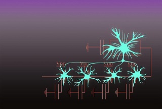
Mapping Deep Learning Algorithms to Neuromorphic Hardware Architecture The ever increasing data volume, velocity, variety, and veracity, known as ”four V” has posed pressing de- mand for a powerful computation platform. The size of data is growing at an unprecedented rate and is predicted to reach 35 ZB by 2020, the so called big data. The Traditional computing platform based on Von Neumann architecture can not deal with emerging computation demands due to the end of Dennard scaling and the serious limitations of Von Neuman architecture known as power and memory walls. In the emerging computation architecture, computation units should be placed in close proximity to data, the so called In- Memory-Processing (IMP) architectures. On the data processing algorithm front, the key issue is to extract valuable knowledge from big data for services support prediction. Deep learning algorithm that can efficiently extract valuable knowledge from big data has gained researcher attentions in recent years. The main issue again is that the Von Neuman based architecture is not an efficient platform to provide the performance needs of big data processing. Neuromorphic computing architecture that mimics the computation paradigm in human brain has gained lots of attention in recent years as an alternative to Von Neumann architecture. We see the brain as integration of billions of neurons, as processor units, surrounded by thousands of synapses for each neuron, as memory units. This view reflects the definition of in-memory processing. In-memory processing not only introduces fast memory access due to the entanglement of processor and memory unit, it also induces the fact that each processor unit only does one or few simple tasks, a fact that is due to the abundance of processing units within the architecture that is massively parallel and requires not much of space as does a warehouse scaled supercomputers that would do the same job with much less speed. Neuromorphic processors are the best candidates that implement this idea as to work similarly to an organic brain. There are lots of researches done in the field of Neuromorphic computing, customizing the idea from different aspects. There are three aspects that interests us in our research. One aspect is the architecture of the processor performing Neuromorphic computing. There are Neuromorphic platforms that closely simulate the brain, so called Biologically plausible processors, such as BrainScaleS project. These types enable complex neural behavior with limited numbers, However, the number of neurons per chip will not be that much compared to an organic brain. On the other side, there are Neuromorphic processors with high number of neurons with a simple computational behavior. IBM’s TrueNorth processor is a known example of these types of Neuromorphic processors. Another aspect is to define the building blocks used in the implementation of a Neuromorphic processor. There are some research works that define the behavior of the memories in a Neuromorphic processor. A memory cell in an organic brain has non-volatile behavior. A synaptic gap that defines memory in the brain is dynamically resistant to incoming pulses. The resistance of the gap reduces as pulses regularly pass through a synaptic gap. Researchers have proposed utilizing different memory devices such as memristors, phase change memories and magnetic memories to implement the similar behavior of an organic memory cell. In addition, the usability of Neuromorphic computers is a field of study for many researchers. There are various ongoing challenges in this field, such as programability, applicability, what types of applications a certain Neuromorphic design will support, etc.
In our research proposal, the key aspect is understanding how the morphology of individual neurons, circuits and overall architectures create desirable computations, incorporates learning and development, adapts to local change (plasticity), and facilitates evolutionary change. As there are many big data applications that require processing resources, we will be investigating the results of mapping big data analysis algorithm on a Neuromorphic processor. To this end we have defined two approaches, a system and an architecture level approach. In the architecture level approach, we will look into an efficient architecture that can be well matched with deep learning algorithms. In this level we will also investigate the use of different devices such as Non-volatile memories and their effects to the functionality of the processor. In the system level approach, we will investigate the viability of using an efficient instruction set architecture (ISA). The ISA we will be working on should be well matched with deep learning algorithms. In other words, to provide instructions that are more machine learning oriented than doing only primitive computations. Once we define the Instruction set architecture, we also look for a compiler that would enable the use of a high level programming language to program the processor. To best study the behavior of our processor design, we will develop our own simulator. This simulator will be tailor-made only for our Neuromorphic architecture. In later approaches we will also integrate our programming language with the simulator, enabling us to define programs for the processor without touching the code of the simulator.
Trading Power, Performance and Security for Energy-Harvested Implatable Medical Devices
Students: Ehsan Aerabi, Milad Bohlouli
2016 - 2019
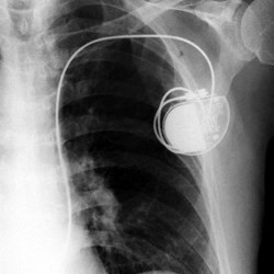
Implantable Medical Devices (IMD) are a category of embedded systems which are placed in a human body to facilitate monitoring and treating chronic diseases. In recent years, IMDs have been equipped with wireless communication which can provide diagnosis data to physicians and receive command and updates from them. This opens the doors for remote attackers. Hence, we need to provide confidentiality and authenticity for the device and the physician's data and commands. To achieve this, we need an extra source of energy for cryptographic algorithms and protocols to involve. Recent research suggest energy harvesting from internal body resources like body movements and blood glucose. This type of energy provides independent power for the IMDs which can send realtime data to/from physician's device. But this source is not a reliable and constant. In this research we try to design a secure communication framework which can utilize the existing harvested energy to achieve the maximum security and throughput. It can reconfigure itself to cope with the limited energy by changing the security and performance parameters. Finding an optimum solution requires a design space exploration among all the apstraction layers in an embedded systems design starting from hardware and architecture to the algorithms and protocols.
Reliable VLSI Circuits and Systems Design
Students: Masoud Katirae, Dadi
2015 - 2019
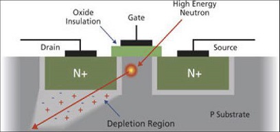
Downscaling of VLSI Circuits into the nanometer regime has brought major reliability challenges. Reduction of threshold voltage, supply voltage and internal node capacitances due to shrinking of feature size, ever increasing of complexity, and operating frequency are the main cause of the reliability issues in Nano-scale technologies. Radiation induced faults, the so called soft errors, are one of the serious reliability threat in nanometer digital circuits. Two reasons make the soft error becoming a major threat to reliability of nanometer digital systems: (1) nodal capacitance is down-scaled and the charge of the capacitance can be affected even with low energetic particles. (2) An energetic particle can affect two or more physical adjacent nodes in the layout and causes multiple faults. To protect a VLSI circuit against soft error, two steps are required including: 1) soft error rate estimation to identify the most vulnerable components; 2) soft error protection of must vulnerable components considering other design objectives like power consumption and performance.
Several methods have been proposed to estimate the soft error rate of digital circuits in recent years. The straight forward method to estimate the soft error rate is Monte Carlo simulation based fault injection. Although, very precise results can be achieved, the execution times of such simulations are intractable for large scale circuits. To address this issue, Statistical Static Timing Analysis (SSTA) based methods have been proposed. These methods are very fast and mostly have comparable accuracy to fault injection methods. However, emerging reliability threats including: (a) The single particle strike and multiple transient faults (b) Process Variations (c) aging effects have remarkably reduced the accuracy and even applicability of previously proposed SSTA based methods. The aging and PV impact on gate delay model and affect timing masking and logical masking mechanisms. In recent years, some research work has been devoted to taking into account the effects of PV and aging separately, however, the joint consideration of both should be performed to have an accurate SER estimation.
In addition to soft errors, as mentioned above, aging effects and process variations are the emerging and important reliability threats in Nano-scale VLSI technologies. There are some various sources of aging induced MOS parameters variations, such as negative and positive Bias Temperature Instability (BTI), Hot Carrier Injection (HCI), and Time Dependent Dielectric Breakdown (TDDB). However, among these sources, the BTI has become the major reliability issues in nanometer MOS devices. Negative BTI (NBTI) in PMOS transistors and Positive BTI (PBTI) in NMOS transistors cause a threshold voltage shift (∆V_th) when they are in the stress phase (ON-State), at elevated temperatures. When PMOS transistor is negatively biased (stress phase) i.e. V_GS=-V_DD, the interaction between the inversion layer holes and the hydrogen-passivated interface Si atoms breaks the Si-H bonds along the substrate-oxide interface. The H atoms can combine to form H_2 molecules and diffuse away (through oxide), then interface traps are generated. These donor-like traps can capture holes and generate bulk oxide traps, giving rise a net positive charge in the gate oxide. The end result is a shift in the threshold voltage of PMOS transistor. By removing the biased voltage, the hydrogens near the interface diffuse back and anneal dangling bands which reduces the number of interface traps and mitigates the NBTI effect (recovery phase). However, this cannot eliminate all the traps, and in long term the threshold voltage increases which in turn results in gate delay increase. Briefly, in presence of NBTI, the delay of a gate increases as it ages. A similar mechanism can be described for NMOS transistors as well (PBTI). In technology size above 90nm, NBTI in PMOS transistors was more significant than PBTI in NMOS transistors and the PBTI was considered to have a negligible effect, however, due to use of high-k dielectrics to reduce gate leakage, PBTI effects have become comparable to NBTI effects.
The PMOS/NMOS I-V characteristics are function of transistor parameters like initial threshold voltage (V_th0), effective oxide thickness (EOT), effective width (W_eff) and effective length (L_eff). In nanometer CMOS technology, precise control of critical dimensions and the other parameters such as channel doping density is very difficult. This results in a large variation in transistor parameters within and across dies. These variations are a consequence of random dopant fluctuations (RDFs) and photolithographic process deviations such as line edge roughness (LER). In particular, variations in Channel doping density, oxide thickness, channel width and length significantly impact on transistor characteristics and accordingly circuit performance. Process variations and aging effects impact on the timing behavior of circuits, as the delay of a CMOS gate is not a deterministic parameter and increases with time. In fact, a gate delay is firstly not a constant value and increases over time due to aging effects, secondly, it is a statistical parameter due to PVs. In fact, the gate delay is a time-dependent and fabrication-dependent parameter due to BTI and PV. As a result, process variation and aging effects should take into account in circuit timing analysis. In this research project, we intend to design a Gate-Level soft error rate estimation methodology based on Statistical Static Timing Analysis considering the effects of process variations and ageing.